Thermal Deposition System is a type of Physical Vapor Deposition (PVD) system used to create thin films by heating a solid material in a high vacuum environment until it vaporizes. The resulting vapor then travels and condenses onto a substrate, forming a solid thin film.
High Vacuum Environment: The process takes place in a vacuum chamber, typically maintained at pressures below 10−5 Torr (and often much lower, e.g., 10−9 Torr). This high vacuum is crucial to ensure that the vaporized material travels unimpeded to the substrate without significant collisions with residual gas molecules, which could lead to impurities or scattering.
Heating the Source Material: A solid source material (in the form of pellets, wires, or a bulk piece) is placed in a heating element. Common heating methods include:
Resistive Heating: An electric current is passed through a resistive element (like a tungsten filament, boat, or basket) that holds the source material.
Electron Beam (E-beam) Evaporation: A high-energy electron beam is directed at the source material, heating a localized spot to a very high temperature, causing it to evaporate.
Flash Evaporation: A fine wire or powder of the source material is continuously fed onto a hot ceramic crucible or heating element, causing it to evaporate almost instantly.
Vaporization and Transport: As the source material is heated, its vapor pressure increases, and it transforms into a vapor cloud. In the high vacuum, these vaporized atoms or molecules travel in a relatively straight line (line-of-sight) from the source to the substrate.
Deposition and Film Formation: When the vaporized material reaches the cooler surface of the substrate, it condenses and solidifies, forming a thin film.
Key Components of a Thermal Deposition System:
Vacuum Chamber: The sealed enclosure where the deposition process occurs, designed to achieve and maintain high vacuum levels.
Vacuum Pump System: Consisting of roughing pumps (e.g., rotary vane, dry scroll) and high vacuum pumps (e.g., turbomolecular, cryogenic, diffusion pumps) to evacuate the chamber and maintain the required vacuum.
Heating Source: The mechanism used to heat the source material (resistive filament, electron beam gun, etc.).
Source Material Holder: Crucibles, boats, or filaments designed to hold the material to be evaporated.
Substrate Holder: A fixture to hold the substrate(s) in place, often with rotation or tilting capabilities for uniform deposition, and sometimes with heating or cooling options.
Power Supply: To provide the necessary current for resistive heating or high voltage for electron beam generation.
Deposition Rate and Thickness Monitor: Devices like quartz crystal microbalances are commonly used to monitor the deposition rate in real-time and control the final film thickness.
Pressure Gauges: To monitor the vacuum level within the chamber.
Shutters: To control the deposition process by blocking or unblocking the vapor stream.
Types of Thermal Deposition Systems:
While the basic principle is the same, systems are often categorized by their heating mechanism:
Resistive Thermal Evaporation: Uses resistive heating elements (boats, filaments, baskets).
Electron Beam (E-beam) Evaporation: Employs an electron beam to heat the source material.
Flash Evaporation: Continuously feeds material onto a hot surface for rapid evaporation.
Applications of Thermal Deposition Systems:
Thermal deposition is a versatile technique with widespread applications across various industries:
Electronics:
Depositing metal contacts (e.g., aluminum, silver, gold) in semiconductors, OLEDs (Organic Light Emitting Diodes), and thin-film transistors.
Manufacturing solar cells (e.g., CIGS solar cells).
Creating interconnects and bonding layers.
Optics: Producing anti-reflective coatings on lenses.
Creating mirror coatings.
Applying protective layers (e.g., UV or infrared light protection).
Consumer Packaging:
Depositing thin aluminum films on plastic packaging to create barrier layers for moisture and oxygen, extending shelf life for food products.
Decorative Purposes:
Applying aesthetic metal finishes to jewelry, sporting goods, and other consumer items.
Materials Science and Research:
Fabricating various thin films for studying new materials and their properties.
Creating multi-layered structures and complex designs.
Specialized Industries:
EMI/RFI shielding.
Light reflectors.
Certain aerospace and medical applications.
Advantages:
High precision and control over film thickness.
Suitable for a wide range of materials, including metals, alloys, and some organic compounds.
Minimal contamination due to the high-vacuum environment
Relatively simple and cost-effective compared to some other PVD methods.
Allows for co-evaporation of multiple materials to create alloys or multi-component coatings.
Limitations: Primarily a line-of-sight deposition process, which can lead to poor step coverage on complex 3D structures. Limited to materials that can be evaporated at achievable temperatures without decomposing. Adhesion between the film and substrate can sometimes be an issue for certain material combinations.
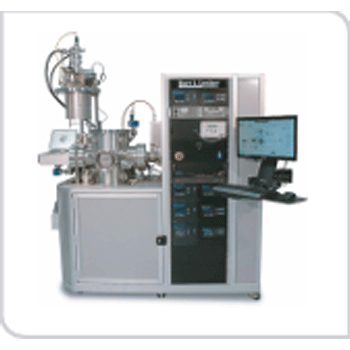
 Atomic Force Microscope AFM
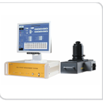 Hall Effect Meserment System
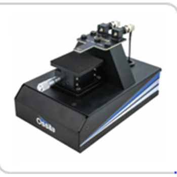 Four-Point Probe
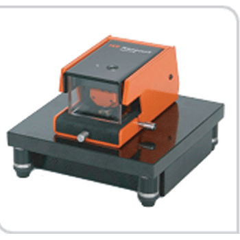
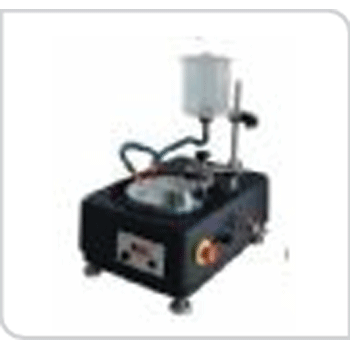 Polishing & Grainding Machine
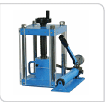 Lab Press With Hydraulic Pump
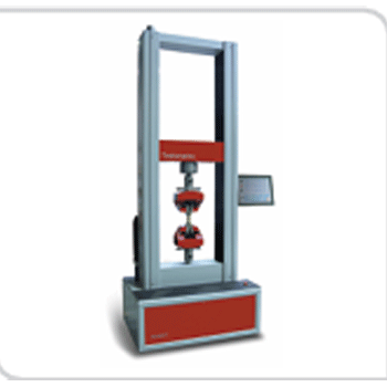 Universal Tensile Tester (UTM)